

Samsung Foundry Forum 2024: Roadmaps
Samsung Foundry Forum 2024: Roadmaps
Getting on Track

One of the super fun events pre-pandemic were the Samsung Foundry Forum annual disclosures. Nominally an event for partners and customers, each year there would be a small press contingent in attendance and a few on the record presentations. During the pandemic this was shelved, and it's taken some time to come back in full force - this year it was held at Samsung's San Jose R&D head quarters, with several hundred people, over companies in the partner area, and additional presentations by Arm CEO Rene Haas and Groq CEO Jonathan Ross.
In typical Foundry fashion, this year was as standard - we're talking about 200 slides swiped through at super high-speed, and no photography allowed (one Foundry is bucking this trend, so I'm hoping they will all follow). I did my best to scribble notes during the open portion of the event.
The key element with an event like this for Samsung is to realign industry expectations on where the company is in its competitiveness and volume offerings. It's hard not to notice when partners are selecting the competition for their latest and greatest AI chips, however Samsung is hope to a number of high-performance designs from AI startups, automotive customers, smartphone, and the company has an extensive base of legacy process nodes vital in power, high voltage, and RF solutions.
Samsung's highlight announcement of the event is the roadmap to its SF2Z process node. That's 'SF' for Samsung Foundry, '2' for 2nm class, and Z means backside power delivery. SF2Z will be the node that integrates that generation's Gate-All-Around technology (which Samsung calls MBCFET), and then BSPDN for additional performance and power efficiency. Some details were given which we'll get into, but the key date here is 2027 - Samsung expects to offer mass production at that time of SF2Z. This will be after the company has mass production of a lot of other SF2-class nodes. SF1.4, the one beyond that, will start risk production in 2027 as well.
Samsung Foundry: Expanding
In light of the CHIPS Act monies heading Samsung's way, it's important to set the baseline as to where Samsung's facilities are. The bulk of the legacy and leading edge is all in Korea, across three cities:
Giheung, Line 6, 65nm-350nm: Sensors, Power IC
Giheung, Line S1, 8nm: Smartphone, Datacenter, Automotive
Hwaseong, Line S3, 3nm-10nm
Pyeongtaek, Line S5 Phase 1 + Phase 2
Pyeongtaek, Line S5 Phase 3 under construction
Samsung also has two sites in the USA:
Austin (TX), Line S2, 14nm-65nm: Smartphone, Datacenter, Automotive
Taylor (TX), 4 fabs announced, space for 10. Will include SF2, SF4, FDSOI, Packaging
Samsung's packaging facilities today are in Korea but also with a heavy leverage of OSAT partners worldwide. The Taylor expansion is set to be the biggest the company has enabled outside Korean borders, and the plan is to offer a full operation on-site for any US business without the need to use Asia.
Manufacturing Technology Roadmap
As with other foundries, Samsung relies on a series major family process nodes, from which there will be a number of variants spawned. In this case, the head nodes are SF4 and SF2.
SF4 Family: FinFET
2021: SF4E (E = Early)
2022: SF4
2023: SF4P (P = Performance, for Smartphone)
2024: SF4X (X = Extreme, for HPC/AI)
2025: SF4A, SF4U (A = Automotive, U = Ultra)
Samsung's SF4 is still a FinFET node and has actually proved to be very popular when it comes to smartphone chipsets and a large number of AI startups that want something leading edge. SF4P is mostly aimed at the smartphone space with lower leakage than SF4, while SF4X is what most of the AI and HPC users will end up on. For anyone looking at mid-range GPUs in 2024/2025, if they're built on Samsung, then SF4X is your best bet.
Due to the higher demands of automotive node requirements, Samsung typically enables an automotive specific version of its technology, and this is where SF4A comes in. SF4U, while it says Ultra, is designed to be a higher value variant of SF4P, showcasing a more premium strategy for smartphone chipset manufacturers that want the benefits of the node improvements but with slightly more headroom and effective production.
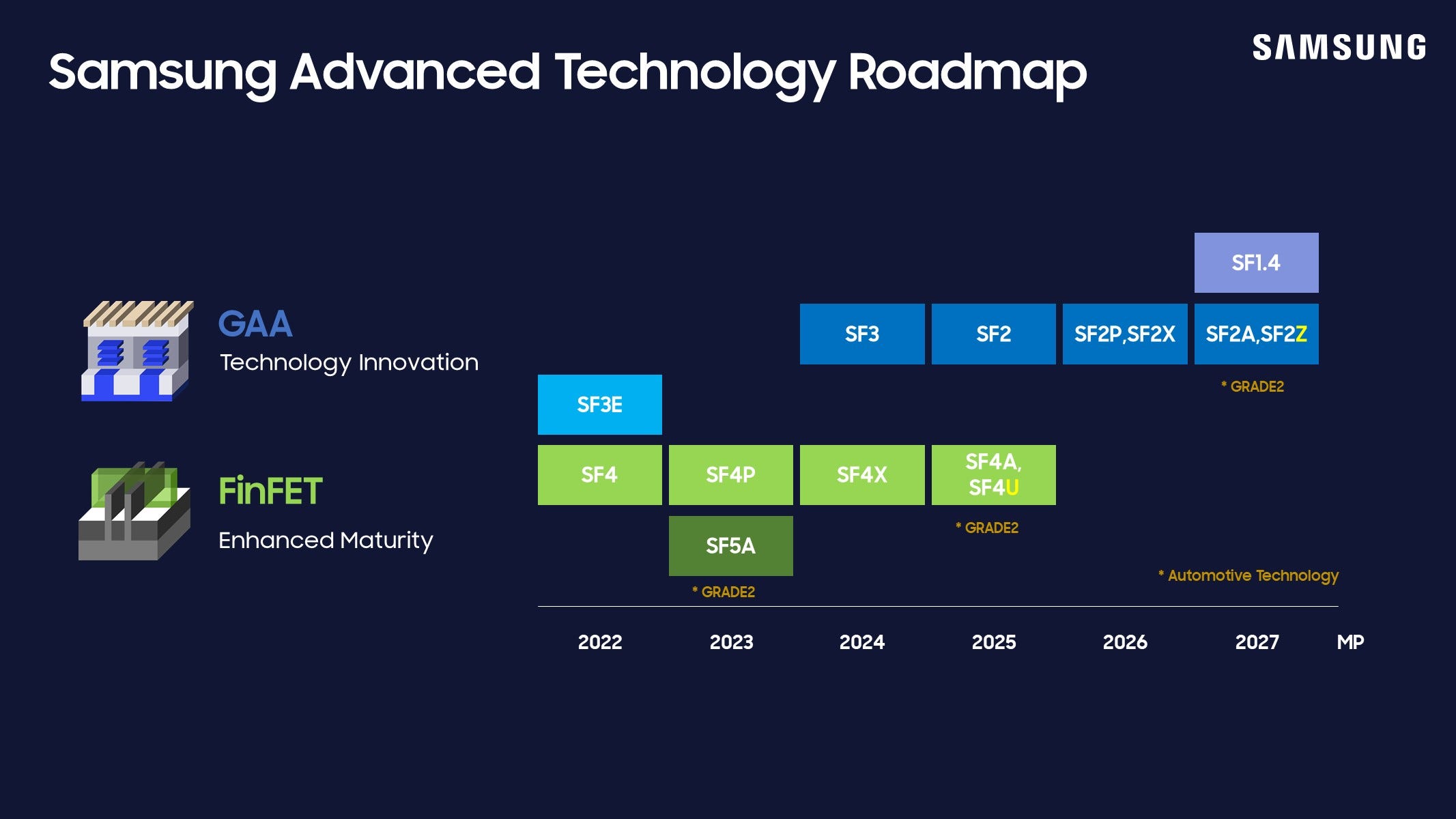
SF2 Family: MCBFET (GAA)
2022: SF3E
2024: SF3
2025: SF2
2026: SF2P, SF2X
2027: SF2A, SF2Z
So this is where it might get a little confusing. Samsung Foundry announced it was the first to production of GAA technology with its SF3E node - appropriately named 'early'. As far as we can tell, while this has been in mass production since 2022, it has been purely an internal node to help develop the technology. Intel isn't set to introduce GAA until its 20A/18A nodes in 2025, while TSMC is looking at N2 in a similar timeframe. Both of those companies are hoping to bring it to market quickly, rather than start with an early announcement like Samsung.
SF3 is the second generation GAA, which is already in mass production in 2024. This might see some pickup, but it's the third generation SF2 which is going to be marketed heavily to customers. Users who follow Samsung might notice that the jump from SF3 to SF2 in the naming scheme is a bit odd - it effectively means that Samsung has renamed its SF3P and beyond family as SF2, likely to better align with the naming used by Samsung's competitors. The argument is as always to competitively align, but that the real customers do know what the performance is, regardless of a node name.
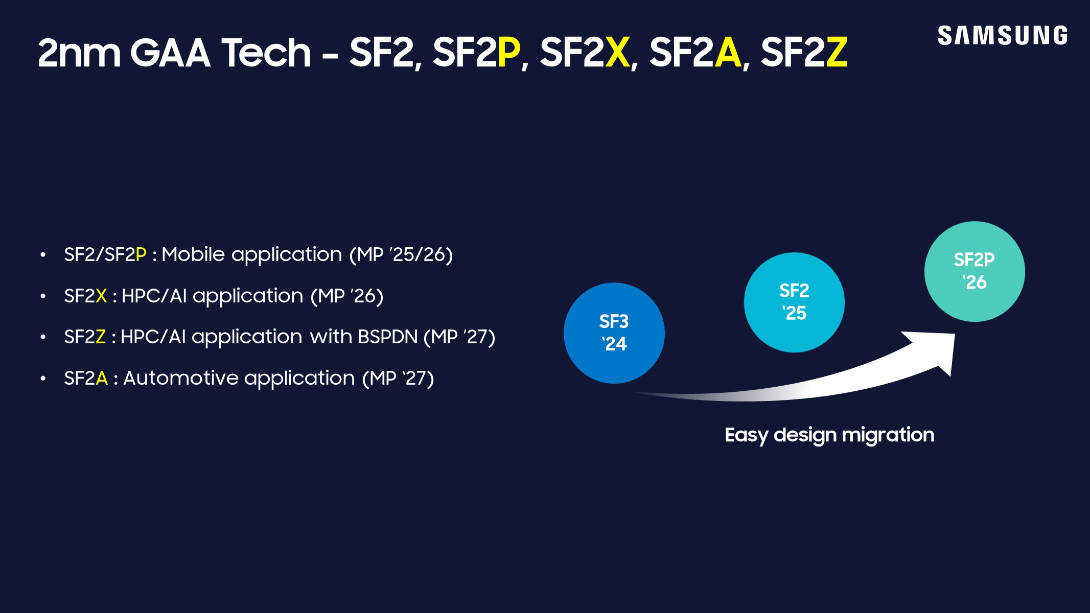
In 2026 we'll see mass production of the smartphone (SF2P) and AI/HPC variants of GAA (SF2X), and here we're following the strategy from the SF4 family pretty closely. In 2027, we get that automotive variant, but it's SF2Z that brings BSPDN to the table. Judging by the discussions at the event, 2027 for SF2Z is a mass production date, not just a risk production hopeful date. That would mean SF2Z risk production would start late 2026 or early 2027, firstly in Korea, before being moved over to the USA in due course.
It's worth noting here that Samsung expects GAA power improvements to be on a better cadence than FinFET - one slide in the deck showcased that planar transistor power (pre-14nm) trended at 0.8x per year, whereas during FinFET the trend was 0.85x/year. Samsung expects GAA to return those improvements to 0.8x/year with GAA / MCBFET.
Plenty more was said in the NDA section, but unfortunately I can't disclose any of that just yet.
Memory Roadmap
Samsung was keen to note its position in the memory ecosystem - mostly as the #1 supplier. The company showcased it has held the #1 DRAM spot since 1992, currently at 41% market share; the #1 NAND spot since 2002, currently at 32% market share; and the #1 SSD spot since 2006, currently at 37% market share. Samsung sees the market as a pyramid.
Tier 1: SRAM
Tier 2: LLC
Tier 3: HBM3E / HBM4
Tier 4: LPDDR6 / LPDDR5X-PIM / LPCAMM
Tier 5: CMM-D (C)
Tier 6: PBSD / CXL-H (C)
I found this interesting in of itself as it showcases some of the upcoming technologies that Samsung is working on. We know that memory standards improve over time, such as HBM3 to HBM4, or LPDDR5 to LPDDR6, but here it shows that Samsung is enabling processing in memory with its LPDDR5X product line. Processing-in-memory is something Samsung has spoken about for a number of years, initially focusing on the HBM stacks and used in partnership with AMD Xilinx FPGAs or custom chip configurations. The fact it's coming to variants of LPDDR5X is substantial, especially if that means there's a benefit to AI in the medium-to-long term to save power. Also on Tier 4 is LPCAMM, the upcoming standard that made waves at Computex (I expect to have a video on my YouTube channel about this later this week). The last two tiers are all about memory and storage expansion, especially with upcoming CXL standards.
The focus for most people on the edge of their seats however is the HBM side of things. Samsung gave insight into some of its numbers, and timelines:
2022: 8-Hi stack HBM3 at 900 GB/sec
2024: 12-Hi stack HBM3E at 1178 GB/sec
2026: 16-Hi stack HBM4 at 2048 GB/sec
2028: HBM4E
I also had time to scribble down a lot of the numbers for HBM4.
Die Density: 24 GB
Capacity: 48 GB/cube
Data-width: 2048-bit (up from 1024-bit)
Pin speed: 6 Gbps/pin (down from 8 Gbps/pin)
Stack Height: 720 micron (no change)
Bonding: Copper-to-copper hybrid bonding (update from previous methods)
Base Die: Includes Buffer, Transition from Planar FET to FinFET
Samsung listed HBM4 as offering 200% speed at 70% area and at half the power. But that's not the end of the story, as Samsung expects custom HBM to be a norm for the most high-performance hardware. This means that the base die, which contains logic and the buffer, to be individually configured by the customer depending on their performance profile requirements. It means that the same HBM4 could be read optimized, or support more memory encryption modes. In combination with a more leading edge base die, the goal is to extract performance and increase efficiency, two hallmarks of the AI crowd that will consume HBM4 like no other.
I really wish I'd had more time to write down everything on the memory slides. It's just as fast paced as the AI market itself at times.
Packaging
One of the areas that Samsung hasn't been promoting heavily, at least from my perspective in the past, has been the packaging side of the business. While other foundries promote CoWoS and EMIB/Foveros, it might be a stretch to even name what Samsung's packaging capabilities are, with or without a marketing name to head it all. Nonetheless, Samsung does participate in advanced packaging, both for smartphone and for AI accelerators.
In the smartphone space, the roadmap looks like this, with the respective thermal resistance ratios
2016: I-POP, 1x TR
2018: FOPLP, 0.85x TR
2023: FOWLOP, 0.85x TR
2025: FOPKG-SIP, 0.65x TR
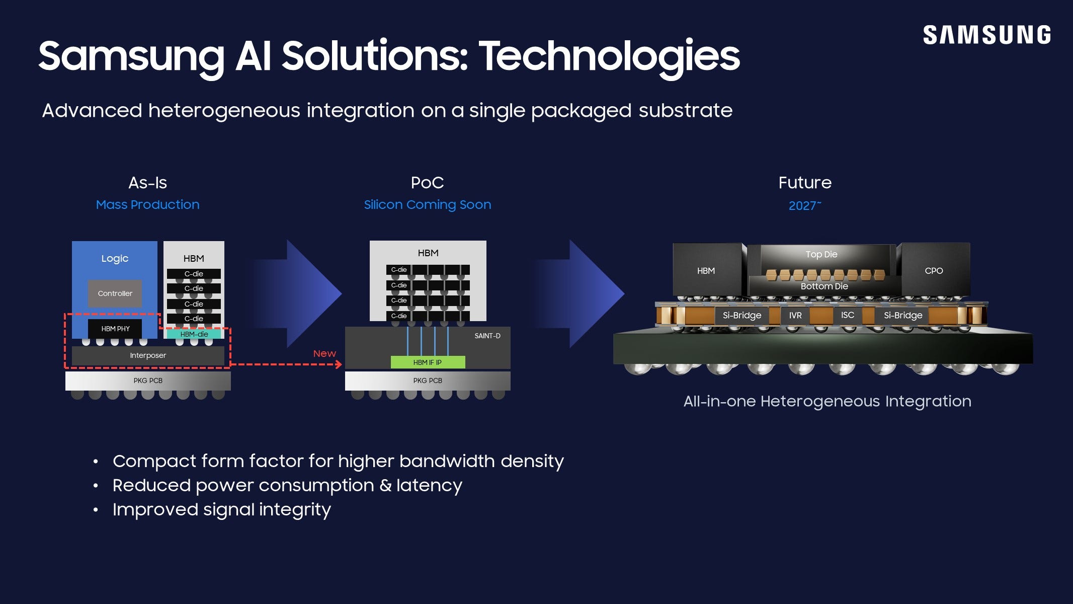
On the AI side, Samsung laid out the following roadmap of what an AI chip should look like.
Today: 2.5D interposer, six HBM3, 80 GB capacity, a bandwidth of 3.35 TB/sec
2024: 2.5D interposer+, eight HBM3E, 192 GB capacity, a bandwidth of 6.6 TB/sec
2026: 2.xD with RDL+Si Bridges, 8-12 HBM4, 576 GB capacity, a bandwidth of 30.7 TB/sec
2027: 2.xD+3D, logic/logic and logic/memory. 16-24 HBM4E, a bandwidth of 70.5 TB/sec
That last one didn't list a capacity, but we're talking about combining 2.5D and 3D capabilities - essentially bonding multiple AI accelerators together. This could be considered something similar to Blackwell, if the base design had one compute die and four HBM3E stacks. But Samsung's thought here is akin to putting two Blackwells together. No mention of power consumption of these ASICs of course!
In terms of 3D integration, we did have some roadmap on when Samsung will have different base die/top die support.
Top Die: SF2 in 2025, SF1.4 in 2027
Bottom Die: SF4X in 2025, SF2P in 2027
This looks like a statement for compute on compute, rather than cache on compute, or compute on cache.
Samsung also dipped its foot into mentioning co-packaged optics (CPO). The company is investing in a CPO strategy, involving a electrical interface chip (EIC), a photonics interface chip (PIC), and optical plates for quick data transfer. I spoke to one of Samsung's optical engineers outside of the presentations and we discussed waveguides in silicon as a longer term solution to bringing lots of chiplets together - if you're familiar with startup Lightmatter's Passage, that enables multiple chiplets to talk to each other with light through a package, we discussed that as a potential future for this technology. Today, most CPO solutions are using GlobalFoundries' 45nm photonics process, or an imec 200nm variant - so having competition in that space would be good to see. Samsung said they expect to have an EIC/PIC proof of concept soon.
Final Thoughts
Back in late 2019, Samsung Foundry's PR agency sent out invites for an upcoming tour of the facilities. Never having heard of anyone visiting Samsung's fabs, not especially press or analysts, I was extremely excited (also at the time, I think I'd only visited one fab). Unfortunately, COVID got in the way, and everything was cancelled. Since that point, when Samsung was starting to open up, I feel the foundry side closed off during the pandemic very quickly. There were some announcements here and there, but it was kept to partners and customers for the most part. This year was the first Forum where press and analysts were invited, and I believe the general tone was extremely positive from those who went - press or partner/customer alike.
The roadmaps showcase that Samsung is committed, long term, to remaining a leading edge fab. It's one thing to be first, but it's another to get it right. Samsung has a strong local chip design industry - I count at least six AI startups on my list and I know a lot of the mid-sized AI hardware companies are set to use SF4X, including Tenstorrent and Groq. On top of that, an identification of where the market is going in advanced packaging is a bonus, and I'd like to see more public discussion and examples of Samsung's capabilities. The Forum was a good start, and I look forward to our next set of data. I'll have to get quicker at writing though, or convince them to share the slides🙂
Ian, thank you for your detailed article. A couple of quick questions. 1) Is FD-SOI going to ramp in Austin or Taylor? I recall earlier press releases indicating that it would be in Austin. 2) Did they share any details about the new research facility that’s planned for Taylor?
At a broader level, given Samsung’s aggressive commitment to the foundry buisiness, how do you feel about Intel’s chances? Is there really space in the market for 3 leading edge fabs?
Thanks for the article!
Small typo: Pheongtaek -> Pyeongtaek (평택시)
If you have ever been there, the Pyeongtaek campus is just massive.