
Apple Announces A19 and A19 Pro SoCs
Latest TSMC Process, GPU Tensor Cores, Memory Tagging for Security, & More

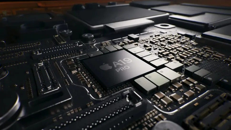
Apple this week took the wraps off of its latest generation of iPhones – the iPhone 17 family – and with it, comes a new generation of Apple’s cutting-edge smartphone SoCs: the A19 and A19 Pro. With access to TSMC’s latest 3nm generation manufacturing process and significant upgrades to the architectures for several of Apple’s functional blocks, Apple is, as always, promising a modest boost in generation-over-generation performance.
Over the years, the smartphone industry has become unique in its high turnover rate in chips. In virtually every other industry, from discrete CPUs to GPUs to FPGAs and more, vendors operate on a two-year (or longer) cadence for replacing their high-end silicon with newer designs. Smartphones and associated mobile devices have become the sole place where we still see yearly chip introductions, with Apple in particular delivering a new chip like clockwork every September of every year. And, in the last couple of years in particular, that has shifted to delivering two chips in slightly different configurations.

All of this goes to reinforce how competitive and how profitable the high-end SoC space is, as it takes significant engineering resources to spit out multiple chip designs per year in this fashion. At the same time, it means that Apple’s engineering teams have to come up with novel improvements year-after-year, regardless of anyone’s opinion of Moore’s Law.
A19 Fabbing: Another Year of Limited Process Gains
The A19 generation marks the third generation of A-series silicon to be produced on TSMC’s 3nm family of process nodes. As TSMC’s historically closest partner (and richest buyer), Apple has often been the first chip designer to get high-volume access to TSMC’s latest process nodes. In the case of the A19 series, Apple has confirmed that they are using the "most advanced 3nm technology,” which, coming from the N3E node used for the A18 generation, we’re interpreting to mean that Apple has shifted over to using the higher-performance N3P node.
N3P is primarily an optical shrink of N3E – coming from tweaks to TSMC’s scanning tools – affording chip designers around 4% better transistor density and either a 5% performance improvement or 5-10% power reduction with otherwise identical hardware. Compared to the A18 series, A19 isn’t identical hardware, but those are still process gains that Apple can invest into improving the performance of their resulting chips.
At this point we don’t have die size or transistor counts for either chip, so we don’t have a good idea of how the A19 series compares to A18 in those respects. Even with the change to the slightly newer node, N3 yields should have further improved over the past year, affording Apple the opportunity to go a bit bigger. But the A-series SoCs are already fundamentally power-limited as it is, so Apple is still constrained in other ways. Given their cache and GPU architecture changes, I expect that the A19 Pro has undergone at least a modest increase in die size and transistor count, but this remains to be confirmed. Meanwhile, any such equivalent increase om the A19 (vanilla) should finally get it over the hump of 15-16 billion transistors that line of chips has been sitting at since A15.
A19 CPU: Improved P-cores, More Cache, & Big Security Upgrades
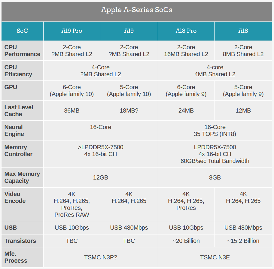
At a high level, the CPU side of the A19 family looks a lot like the A18 family – or the past several generations of A-series SoCs, for that matter. Apple has once again stuck to their tried and true 2+4 configuration, pairing a duet of performance cores with a quartet of efficiency cores. This goes for both the vanilla and Pro versions of the SoCs, so in terms of raw theoretical throughput, both chips are virtually identical.
Apple typically offers the press a bit more insight into their architecture once their products are near launch and journalists are being sent review sample phones. So in lieu of that, we only have some limited high-level information about the changes that Apple has made with this generation of their CPU architecture.
For the performance cores, Apple says that they’ve improved their front-end bandwidth. Apple’s CPU architecture is already famous for how wide it is, so it sounds like this is a change to further help keeping the beast fed, but that remains to be confirmed. Meanwhile, Apple has also made further improvements to their branch prediction unit, which has historically been a common avenue of focus for CPU developers, as cutting down on bad branch predictions – and thus avoiding work that accomplishes nothing – remains a tried and true method of improving CPU performance.
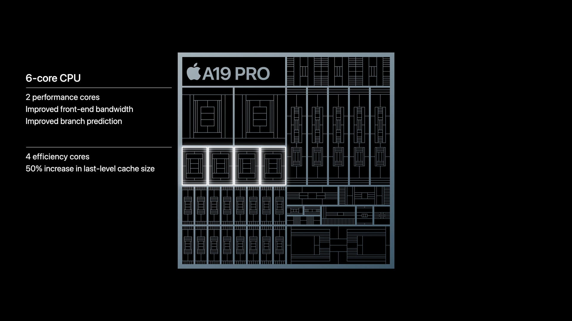
On the efficiency cores, Apple has not outlined any architectural improvements.
However, in the same breath, they have made the unusual claim that they have increased the size of the last level cache (LLC) on the A19 Pro by 50%. As nothing that goes into an Apple keynote isn’t vetted by less than half a dozen people, I’m going to assume there’s no error here – that is, someone didn’t mean to say L2 cache – and rather that Apple opted to comingle any discussion of the entire chip’s LLC into this segment of the presentation. In which case, that means that Apple has increased the LLC from 24MB on the A18 Pro to 36MB on the A19 Pro.
The LLC backstops more than just the CPU cores, but like branch predictor improvements, it’s another generalized change that can improve CPU performance overall, as the LLC is faster to get to than relatively slow DRAM. It also pays some dividends in terms of power efficiency as well (going to DRAM is expensive), though this is somewhat offset by keeping the additional SRAM cells powered.
As for specific performance claims, Apple isn’t offering any peak CPU performance comparisons between A19 devices and A18 devices. The closest thing they offer is a claim of up to 40% better sustained performance for the iPhone 17 Pro as compared to the iPhone 16 Pro, which is likely more heavily reliant on the changes they’ve made to cooling and their use of a vapor chamber there.
Otherwise, the next closest comparison is the iPhone 17 Pro versus the iPhone 15 Pro, where Apple is saying that the CPU is up to 20% faster. And comparisons of the non-Pro iPhones are more favorable, since the vanilla iPhone 15 series used the even older A16 SoC – so Apple is claiming a 40% CPU performance improvement over those phones. Unconfirmed Geekbench numbers from early (and careless) testers looks promising, but we’ll have to wait and see how the confirmed performance numbers compare.
Finally, outside of the usual architectural performance improvements, Apple’s other big investment in this generation of their CPU core designs has been on memory security and resilience against CPU & memory-based attacks. Dubbed Memory Integrity Enforcement, the full scope of the technology goes beyond this hardware-focused news post, but Apple is rolling out several improvements in an effort to put the kibosh on buffer overflows and use-after-free vulnerabilities.
Memory Integrity Enforcement is a multi-layer approach to security, but the big change at the hardware level is that Apple is finally supporting memory tagging, in the form of Arm’s Enhanced Memory Tagging Extension. Intended to circumvent memory attacks by tagging (locking) memory regions, MTE-enabled hardware will block (and typically crash upon) rogue pointers from accessing memory regions they shouldn’t, by virtue of requiring a key to access that memory region.
Arm has been offering memory tagging to its licensees for several years now, and it has already been adopted in parts of the ecosystem. But Apple has opted to wait for the more recent and improved Enhanced MTE to adopt the technology, citing MTE’s lack of protection of non-tagged memory.
Besides implementing memory tags, Apple’s security blog outlines how the company has also worked on the plumbing within their CPU cores to ensure that EMTE tags aren’t then sniffable via side-channel attacks. To that end, while Apple doesn’t block speculative execution when EMTE is in use, they do have it configured such that it won’t influence speculative execution in any way – preventing attackers from isolating valid tags.
While the full contents of Apple’s blog post get into the weeds in a way that few consumers would appreciate, it’s telling that Apple opted to publish this blog post on the same day that the first SoCs supporting the technology were revealed. Giving developers the tools to harden their apps against (and hopefully put an end to) what are now the most common attack vectors on iOS is potentially a huge deal for the company, especially as complex exploits built on top of memory attacks are how most state actors are compromising iPhones these days.
A19 GPU: Apple10 Architecture Features Faster FP16 Ops and Tensor Cores
On the GPU side of matters, the A19 SoCs are introducing a new generation of Apple’s GPU architecture. Already stubbed out in Apple’s developer documentation as Apple10, the A19 SoCs are bringing a few major feature additions that Apple has been teasing developers with since the announcement of the Metal 4 API at this year’s WWDC conference.
From a hardware perspective, the A19 and A19 Pro SoCs aren’t making any wild changes to their GPU configurations. A19 ships with 5 of Apple’s 10th generation GPU cores, while the A19 Pro SoC gets a 6th GPU core. This is the same 5-or-6 configuration as on the A18 series of SoCs.
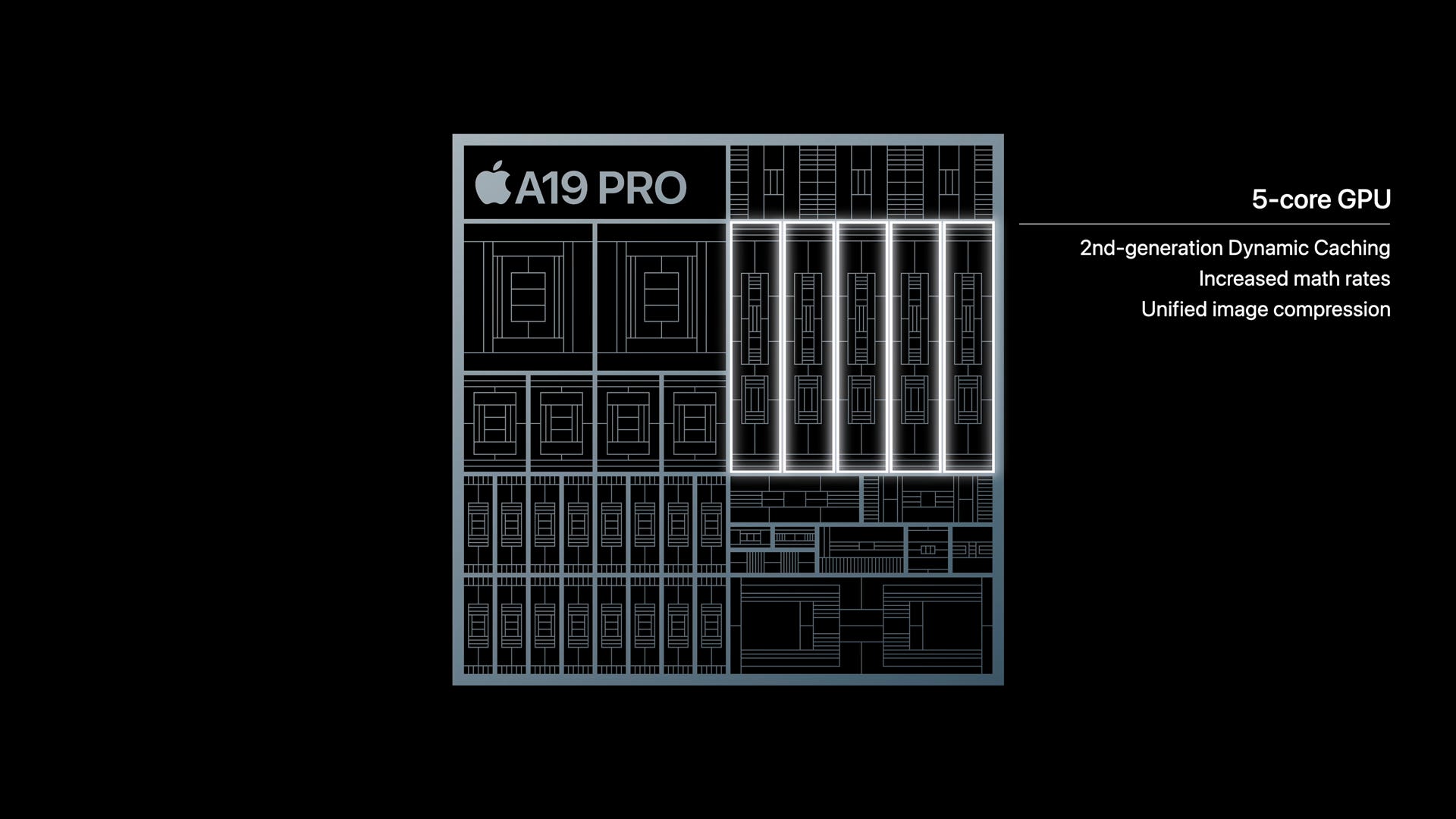
Instead of adding more GPU cores, Apple has opted to beef up their current GPU cores in a few ways.
From a graphics standpoint, the biggest change here is improved FP16 performance. Apple claims they have doubled FP16 performance versus earlier GPU architectures. Assuming all of this is true, and the internal workings match the straightforward explanation, then it sounds like Apple has reversed a curious change in the Apple7 GPU architecture, which reverted on FP16 on a relative basis.
Apple has been promoting the use of FP16 since at least as far back as the A8 SoC (Apple2 GPU architecture), when they added support for FP16 registers, allowing developers to save on power and memory bandwidth by using FP16 datatypes when possible. At the same time, FP16 throughput on Apple SoCs was 2x their FP32 throughput. However FP32 and FP16 performance equalized in the Apple7 architecture, meaning that although using FP16 still saved on register pressure, memory pressure, and memory bandwidth, it didn’t directly unlock further FLOPS.
With the FP16 change for the Apple10 GPU architecture, all signs point to Apple returning FP16 throughput to twice the rate of FP32 throughput. Whether this means they doubled up on the number of FP16 ALUs or are now doing packed-FP16 operations (packing two FP16 ops into a single FP32 ALU) remains to be seen. But either way this should have some performance ramifications for graphics workloads.
More nebulous, the Apple10 GPU architecture also incorporates a newer iteration of Apple’s dynamic caching system. As a reminder, dynamic caching is Apple’s name for their dynamic video memory allocation system, which seeks to avoid allocating more memory to a buffer than is necessary. Apple has never outlined just how it works, but as emphasized that it improves performance as well as reducing register and memory pressure. So a further iteration on this may provide performance benefits, but this remains to be seen.
Apple has also introduced what they’re calling “unified image compression” to the GPU architecture, but with no further details. All major GPUs already make significant use of image/buffer compression to save on cache pressure and memory bandwidth, so it’s largely a question of what “unified” means in this context. Presumably, Apple has made further changes so that all of its units within its GPU can ingest compressed buffers.
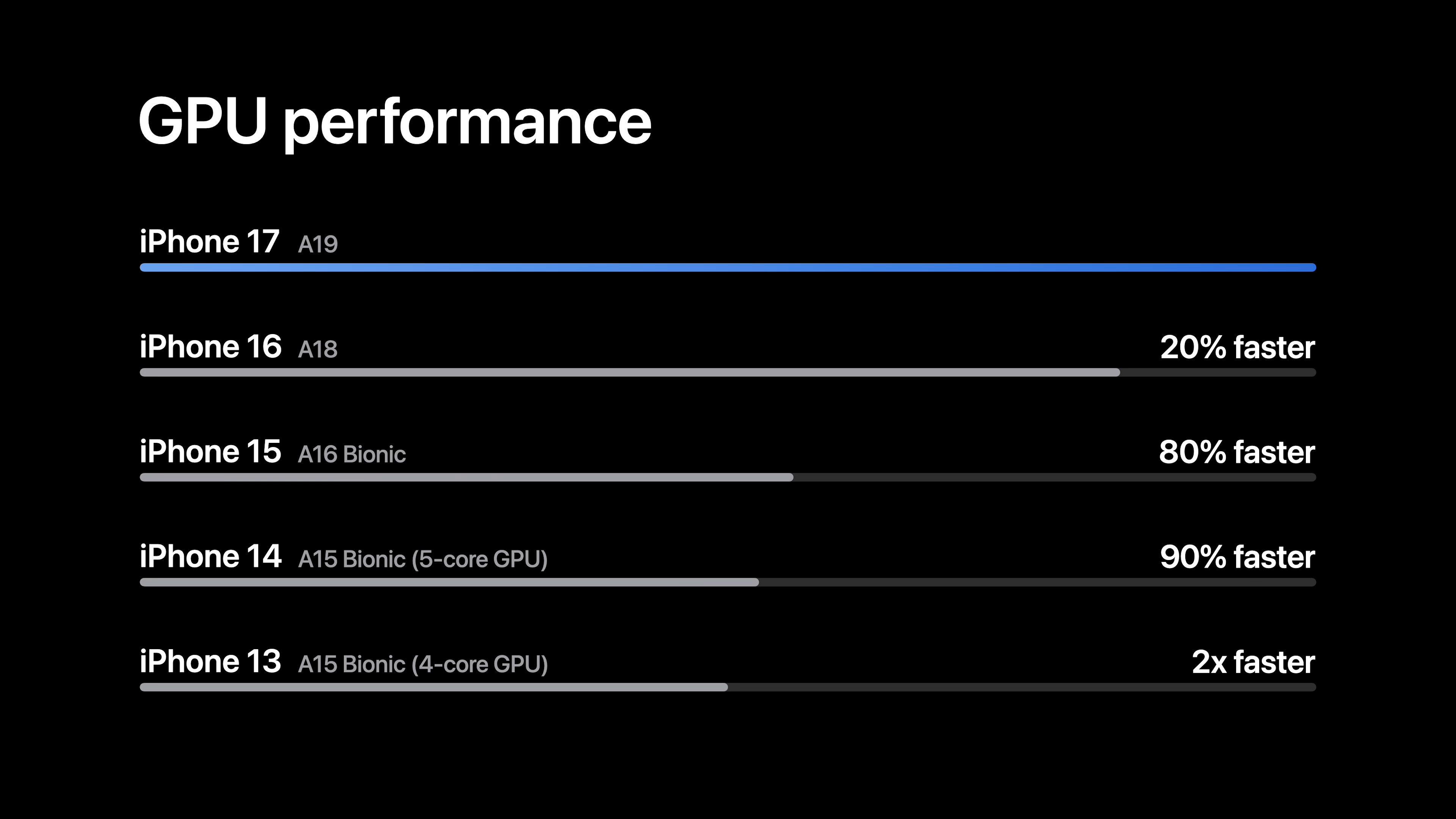
In terms of graphics performance claims, Apple is offering a few different metrics. Comparing the vanilla A19 to last-year’s vanilla A18, Apple is claiming that the iPhone 17 should be around 20% faster in GPU performance than the iPhone 16. Otherwise, compared to the iPhone 15 generation, Apple is claiming that the iPhone 17 is up to 80% faster than the iPhone 15, and the iPhone 17 Pro is up to 50% faster than the iPhone 15 Pro.
Finally, Apple’s other big hardware addition on the GPU side won’t have quite as much of an impact on graphics, but it will be a big deal for its GPU compute users: tensor cores. Or as Apple is calling them, Neural Accelerators.
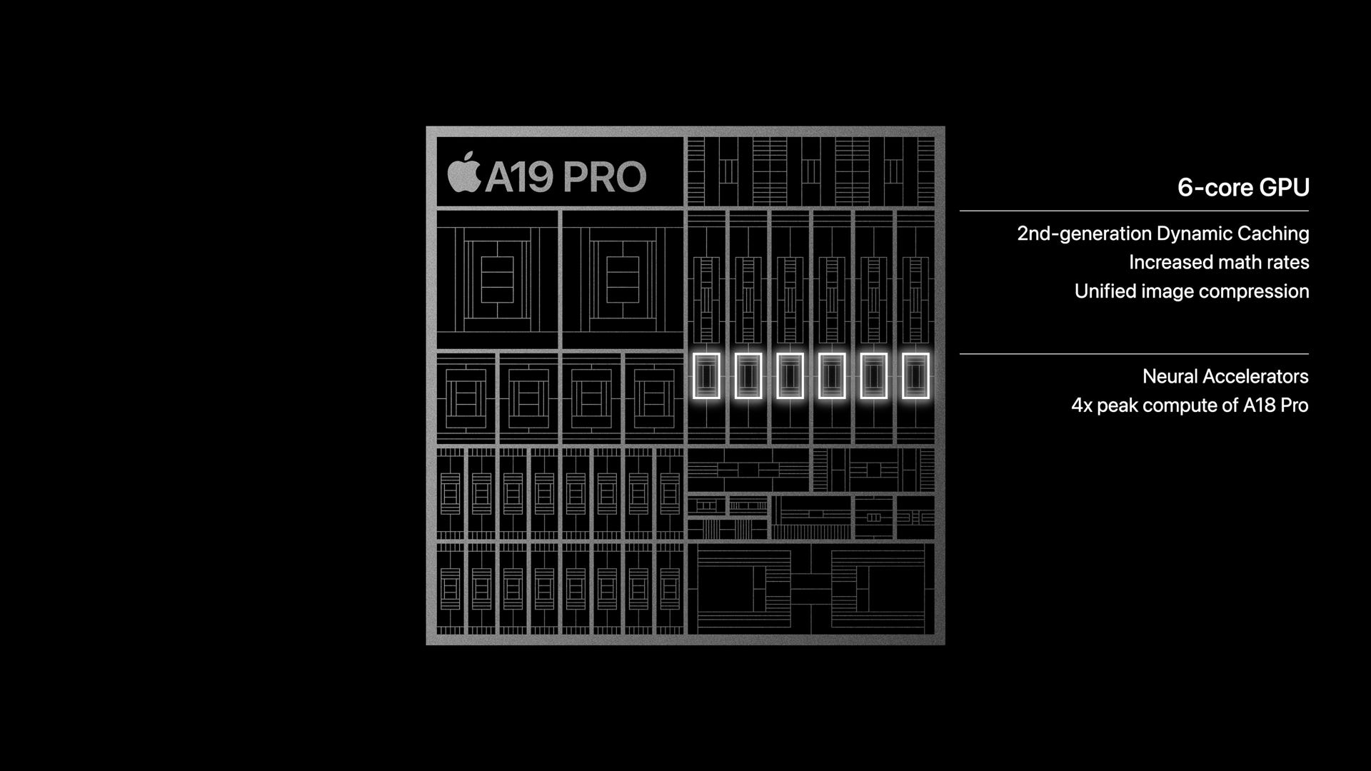
As with the tensor cores on NVIDIA’s GPU architecture, the matrix cores on AMD’s GPU architecture, and similar units on other GPU architectures, tensor cores are highly optimized compute blocks for operating on multi-dimensional arrays of numbers (tensors). Tensors are especially common in machine learning tasks, where tensor cores are used to execute vast matrix-multiplication operations.
GPUs are already powerful matrix-multiplication engines (there’s already plenty of that math in graphics), but tensor cores ramp things up further by increasing the size of the arrays and matrices that are being operated on. The design of these cores is essentially a SIMD on steroids, operating on hundreds of numbers in a cycle instead of a dozen, reducing the amount of hardware required for control flow to a bare minimum while maximizing the number of ALUs available.
Apple previously teased this addition back at WWDC with the addition of tensor support in the Metal 4 API. Metal 4 will actually support tensor operations going all the way back to Apple7 GPUs, executing tensor operations on those GPUs’ SIMDs, but users need an Apple10 architecture GPU in order to get the full performance benefit of using tensors.
Notably, these neural accelerator cores are distinct from Apple’s existing Neural Engine cores, which reside on a separate area of the chip. Whereas the neural engines are for efficient, low-power ML inference, the neural accelerator tensor cores lie within the GPU, and are intended for much higher overall performance. Albeit at the cost of much higher power consumption.
Altogether, Apple is promising that the A19 Pro SoC in the iPhone 17 Pro will offer 4x the peak GPU compute throughput of the A18 Pro, which aligns closely to what you’d expect to see from the addition of dedicated tensor cores. Otherwise, it’s telling that Apple has separate performance claims for the iPhone 17 Pro and the iPhone 17 Air, at 4x and 3x respectively. Those tensor cores are incredibly dense by design, so it’s no surprise that the petite Air is going to have more trouble keeping them cool.
A19 Odds & Ends: Faster DRAM, Updated Neural Engine, ProRes RAW
Rounding out Apple’s 2025 mobile SoCs, there are the remaining functional blocks and other major aspects.
On the memory front, Apple has confirmed that the A19 chips have more memory bandwidth, but not to what degree. The A18 family of chips shipped with LPDDR5X-7500, and a year later LPDDR5X is readily available at speeds over 8000 MT/sec. So it’s all but given that Apple will be using faster memory – the only question is how much faster?
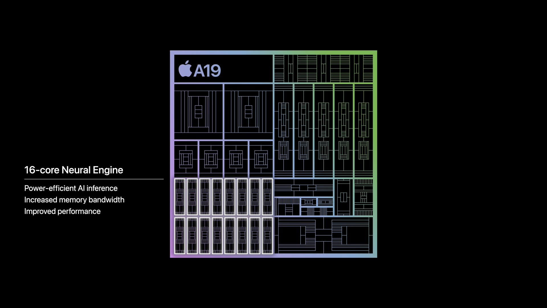
Meanwhile, the A19 chips are also getting a revised Neural Engine block. This block is still comprised of 16 cores, but Apple has touted improved memory bandwidth and improved performance overall. Notably, however, they aren’t offering any performance figures for this generation, whereas they were up-front with their 35 TOPS (INT8) figures for the A18 generation chips. I would expect that major improvements such as new, lower precision formats would be declared up-front, so we’re presumably looking at more subtle changes that improve performance here.
The new SoCs are also getting a new display engine, though Apple isn’t disclosing just what has changed. The bulk of the work seems to be to better support the displays on the newest iPhones, particularly the availability of ProMotion on the iPhone 17.
And while not called out in any of Apple’s slides, the company’s teams appear to have been revising both their ISPs for their cameras, and their associated video encode blocks. Of particular note, the A19 Pro SoC – and only the Pro SoC – has added support for recording in Apple ProRes RAW, joining the previous Pro SoC’s support for regular ProRes. ProRes RAW support essentially doubles-down on Apple’s support for professional video capture formats, with Apple offering their own flair on top of traditional RAW camera formats.
This does widen the gap between the vanilla and Pro SoCs a bit, by adding yet another feature that’s only available on the Pro SoC. At the same time, outside of cache sizes, the bulk of the difference between the A18 SoCs was also in camera/video features, so this continues that trend, with vanilla iPhone 17 users limited to recording in H.264 and HEVC. And while AV1 decoding is supported, there isn’t any support in this generation of chips for AV1 encoding.
Finally, Apple seems to be keeping USB data rates as a further differentiator between the two SoCs. While the A19 Pro-based phones support USB at data rates up to 10 Gbps (USB 3.2 Gen 2, aka SuperSpeed+), the vanilla A19-based iPhone 17 is limited to 480 Mbps USB (USB 2.0, aka High-Speed).
Apple N-series Wireless Networking Chips Makes Their Debut with N1
Finally, while not part of the A-series SoC itself, this generation of iPhones brings one last debut on the Apple platform with the Apple N1 wireless networking chip.
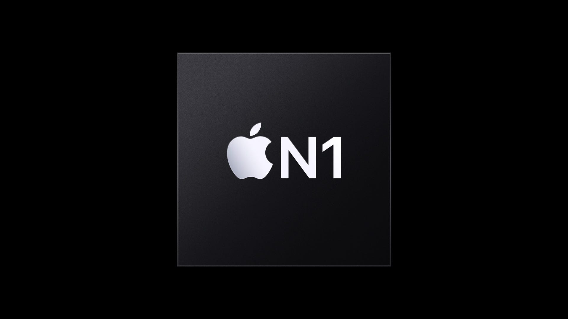
Apple’s first in-house short-range radio chip – not to be confused with either their C-series cellular chip or U-series ultra-wideband chip – the N1 will handle Bluetooth and Wi-Fi support for Apple’s devices, along with Thread networking technology. Prior to this generation, Apple has been a steadfast Broadcom customer, leaning on them for wireless chips for both Macs and i-devices alike. So the shift to their own silicon is particularly notable, as this is one fewer chip that Apple has to source from an external chipmaker to build their own devices.
In terms of high-level specifications, the N1 is pretty typical fare for a high-end radio chip. Apple supports Wi-Fi 7 with up to 2 spatial streams (though not disclosing at what channel widths). Meanwhile on the Bluetooth front, Apple is introducing Bluetooth 6.0 support, bringing last year’s spec into hardware. And while BT 6.0 doesn’t bring any grandiose new features to the table, channel sounding allows for Bluetooth devices to be aware of their distance from each other, which should eventually help to improve Apple’s Find My feature separate from their ultra-wideband tech.
Broadcom’s wireless networking chips have, broadly speaking, been among the best regarded in the industry. So it will be interesting to see if Apple is able to meaningfully improve on Broadcom’s offerings, or if this change is primarily just about bringing that piece of the iPhone puzzle in-house. There is also the potential that this is a Broadcom chip underneath (or through physical design), but with Apple enhancements on top.
Ultimately, we should be getting a better look at the A19 SoCs and their associated iPhones in the coming days. iPhone pre-orders open today, September 12th, which hardware reaching users’ hands a week later, on September 19th.
Here's what I think is happening with the FP16 rate:
https://forums.macrumors.com/threads/apple-silicon-deep-learning-performance.2319673/page-14?post=34127092#post-34127092
I *think* this also covers the "neural cores" claim but we'll see.
As for "unified image compression" I believe this refers to the compression of INTERMEDIATE buffers (g-buffer, bump-map, etc) used to construct a final image.
Obviously imagery that is brought into the GPU as resources (basically "textures" in all their variety) is compressed by everyone. And you can compress material at the very end of an operation, once you know you're done with it.
But compression of intermediate buffers is a tougher project because it's essentially a coherency problem -- as soon as you compress parts of a buffer you now have that "buffer state" is not just spread over multiple caches but also at two different address ranges (the compressed and the uncompressed range). It's tracking all this so that compression happens as the buffer is assembled, rather than as a final additional (and synchronous rather than asynchronous stage) that's the tech part of "Unified image compression".
I've always loved your writing style, Ryan: simple, thorough, and with impeccable grammar (well ok, there was one minor spelling mistake!). I'm glad you've found a new home here.
I also enjoy the re-use of AnandTech's Table colors and styling :-)