

An Interview with Pat Gelsinger
An Interview with Pat Gelsinger
The Road to #2 Foundry by 2030

In February 2024, Intel held its first Intel Foundry Direct Connect event – an opportunity to bring together partners, customers, potential customers, and the media and align everyone with the singular message and vision of Intel Foundry. This means progress reports, updates, and the future. The tone of the event was one of success – Intel Foundry (IF) is set to be a semi-autonomous body of Intel that aggressively fights for business, whether Internal or External, without playing favorites. Similarly, Intel Product Groups (IPG) are being detached from Intel Foundry, with the remit to use the best process nodes available. The whole goal, according to CEO Pat Gelsinger, is to make both sides better for business – built the best process nodes regardless of product, and build the best products regardless of process node. Intel, for the first time, is extracting out the margins between product and manufacturing, in the goal to return to a world leading entity in both categories.
Alongside a keynote from Pat Gelsinger, the event also included presentations from Stu Pann, SVP of Intel Foundry, Q&A with Dr. Ann Kelleher, EVP of Technology Development, and Keyvan Esfarjani, EVP of Manufacturing and Operations. Executives from UMC, Mediatek, and Broadcom also came to the stage, and at the end of the day, Pat sat down with Sam Altman, CEO of OpenAI, to discuss the need for competitive foundry to enable the next generation of machine learning capabilities.
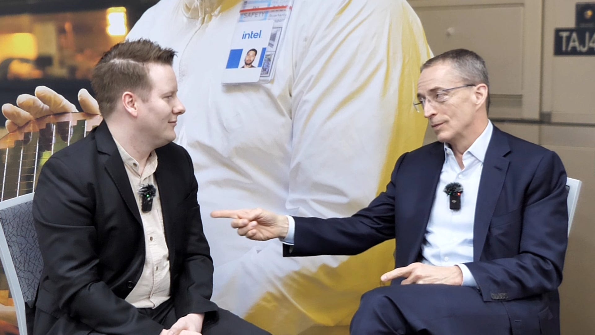
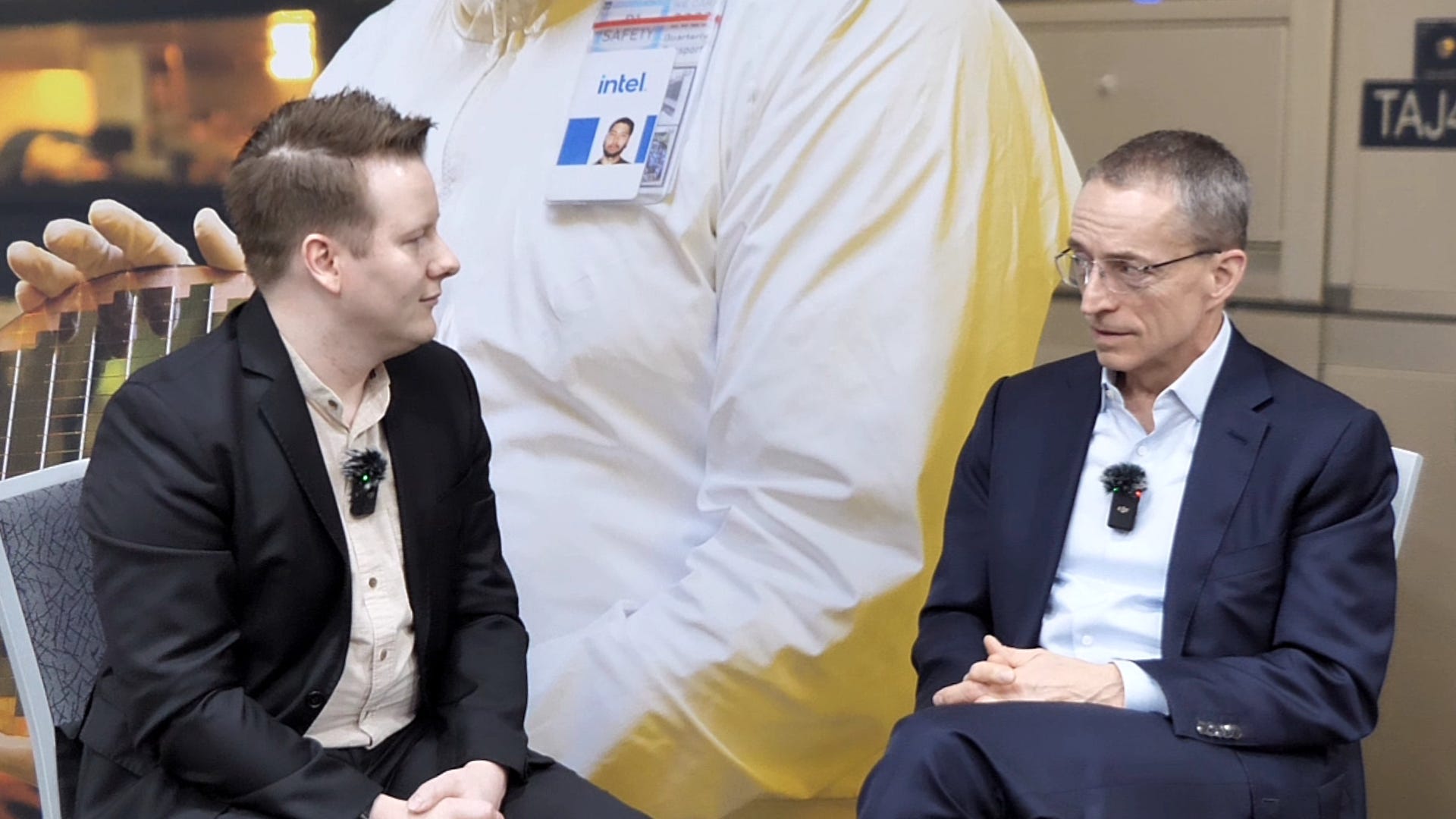
On my flight over to the IF event, with my trusty $35 handed over for 10 hours of 2Mb airline speeds, I received an email from my Intel contacts offering a one-on-one 20 minute interview with Pat at the event. At a company as large as Intel, getting more than 20 minutes with the CEO is a luxury too good to pass up – my only request was to also film it, and you can watch the interview here.
For full transparency, while I am a technology analyst under retainer with Intel (as well as AMD, IBM, Qualcomm, and I’ve done paid work with TSMC), this was not sponsored content or a commissioned review. While the request was to focus questions on the topic of the event, the questions were not shared in advance with Intel or their teams. I solicited questions from industry peers and social groups I’m part of in advance, and wanted to address recent high-profile topics of High-NA economics, divestment of the Foundry Business, and competitiveness against TSMC. All these questions were asked, and answered.
The following is a transcription of the interview. Phrases have been tidied up for readability and clarity. This is not investment advice, and provided as-is.
Ian Cutress: One of the things you’ve presented today is the “road to High-NA” and its integration into your roadmap. One of the comments recently has been about the economics of High-NA - the financial economics, and being able to bring it to market in a cost-effective way for the customers. Simply put, do the economics of High-NA work?
Pat Gelsinger: We’re looking at it pretty carefully of course before I put that much capital at play on a High-NA machine. An EUV machine is ~$250 million, and a High-NA machine is $400 million-ish, so do the economics work? We've looked at it pretty carefully - when you go to double patterning versus single patterning with High-NA. Yeah, we can make the economics work and those associated with it. Now of course you have to get the value of those tighter pitches that you're able to get, but we’re looking at it pretty carefully. We think it pencils out well compared to some of the other multi-patterning techniques and some of the self-alignment techniques that can be done. We think it's going hang together and we're pretty excited about it. Of course, with the field size, that becomes an issue if you go to larger field sizes, I’m challenging both ASML and my mask-making team to get me to bigger mask sizes so we can get the field size back, and maybe even bigger mask sizes to get even more economics out of EUV overall. [There’s] a lot of pressure to make sure the economics work out, because one of the things was as we move through the EUV generation, the economics of Moore’s law stopped. I have to get the economics back into Moore’s law, so it's not just building faster transistors, lower power transistors, but cheaper transistors as well. That’s a big priority for us is make sure the economics of Moore’s Law are on the other side of the EUV transition.
Ian: That’s even with the increased ASP of some of these more advanced packaging techniques? Because those sort of products which will be on the bleeding edge, those will be the ones powering the big machine learning clusters. So we continue the economics of making a cheaper transistor in more expensive products?
Pat: Yes. Fundamentally it’s always a “is it economical?” question. Moore’s Law was a technological statement, but more so it was an economic statement. If I can build products that are faster, use less power, and are cheaper, okay, everybody is going to go there, and that is the magic of Moore’s Law. When you don't have the economics there, then it’s sort of like “eh, if I stay on the current node, I can be more parallel” - which is where a lot of these AI machines go to get their performance capabilities. If I say “hey you've got to move to the more advanced nodes, because you get more performance, and lower power, and it costs less”, then it’s a killer value proposition and we’re in the heydays of the next phase of Moore’s Law. Frankly, I think we’re there, and I think we're going to make that work.
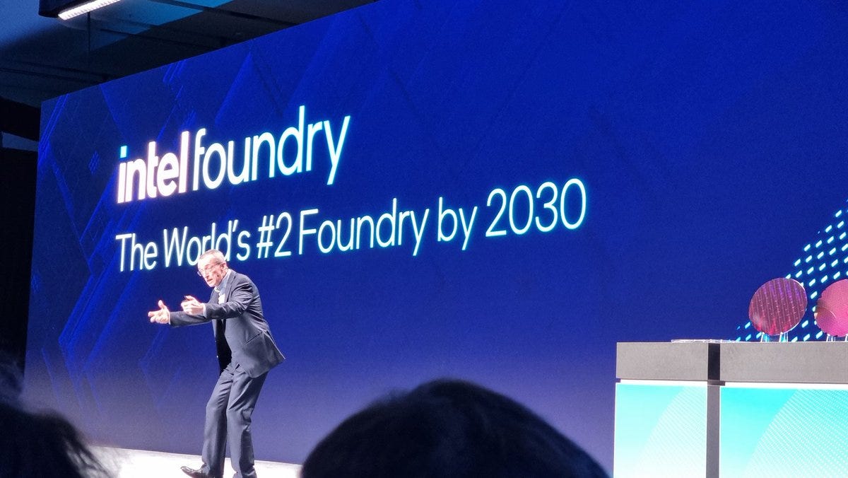
Ian: You’ve said today that you want Intel Foundry to be the #2 foundry by 2030, and yet the rest of the presentation is about how you're a different foundry than everyone else with this whole concept of a systems foundry. On that comment, is that number 2 spot about revenue, wafers, or the performance of end products? What’s the best metric to use, and how far along are you by now?
Pat: Yeah, and explaining that statement a little, I’m already the #2 foundry in the world. If you count internal wafers.
So when I say #2 foundry by 2030, I mean [for our] external foundry [business only].
That is a very substantive statement because we’re saying that we’re going to be, by revenue, the #2 foundry by the end of the decade. That’s the goal that I’ve set out for our team, and that’s above the revenue that I get from the internal foundry business. So it’s a combination from both. I believe it’s going to be a big number by the end of the decade, but we’re trying to be very transparent. I’ll say, appropriately comparable, my external foundry will be #2 in the industry - obviously we expect TSMC to be #1, and by then we’ll have bypassed GlobalFoundries, UMC and Samsung as the #2 revenue foundry in the world.
Ian: Are you including packaging in that revenue?
Pat: Some of it will be advanced packaging, as well. TSMC does the same thing, so we think that’s a fair comparison. We do think that advanced packaging will be well below 50% [of our products/revenue?], but it's going to be a growing piece of the revenue. When you think about advanced packaging Ian, is it wafers or packaging? Increasingly advanced packaging is wafer technologies and wafer level assembly techniques [such as] hybrid bonding going onto silicon-based substrates. So is that more silicon, wafers, or more wafers? In time it will be glass. So with that, we think [adding packaging to revenue] that it’s a fair comparison, saying the advanced packaging is one of the elements. Relationships like UMC and Tower will give us some legacy nodes, and we’ll have advanced packaging, but the majority of that revenue will be leadership with post-EUV wafer revenue.
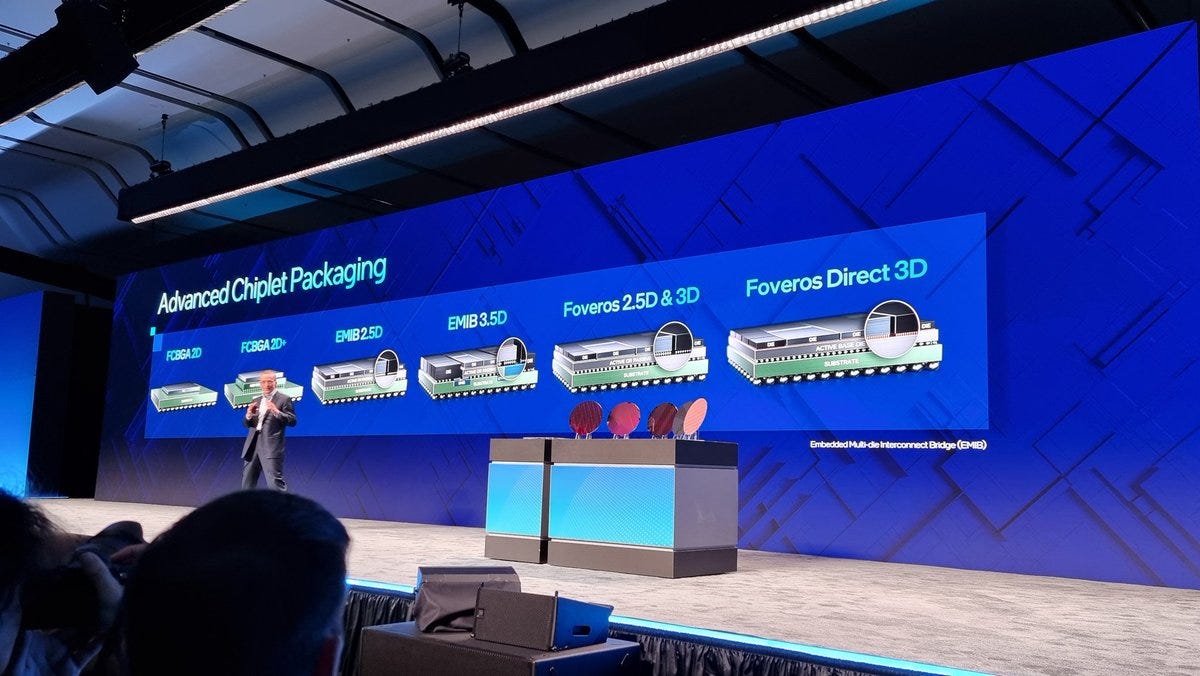
Ian: One of the big drivers in the chip market right now is your competitor TSMC’s CoWoS availability, and their ability to supply. You’ve extensively spoken about EMIB and Foveros, and Intel leading into Foveros Direct. However, what would you say is the comparative competitive technology Intel has against CoWoS?
Pat: Well, Foveros and CoWoS are pretty comparable. They’re a little bit different. Clearly due to some of the supply limitations that you described, some of our advanced packaging customers today are taking Foveros, and we’re helping them to be able to move their CoWoS designs to Foveros. It’s just taken up by supply chain, and ‘hey, you have advanced packaging capabilities’ - we can do Foveros with you. This gives us more volume of our AI chips, and most of these are AI customers, so this gives us what I call the “fast on-ramp” into the foundry business.
But now that we’re starting to work with them, we can start to explain that CoWoS and Foveros are square functions - you're scaling in both the X and the Y, and that’s a pretty expensive base die. If we use EMIB for the high performance bridged connection, that is way more cost effective in a lot of circumstances [than a single large base die], and the customers are starting to look at our packaging technologies. They’re saying “wow, so I can use some for EMIB and some for Foveros and get a more economic and high performance design, that’s pretty interesting”, and then they’re starting to see some of the advanced testing capabilities that we provide. When you're bringing many of these components together onto an advanced package, all of a sudden the individual die or chiplet, and the testing associated with that, becomes very critical in the overall yield of the cost structure of the full complex advanced package. So we do full performance simulated die test, another differentiated capability. Then we tell them about Foveros Direct - now I can do full die-on-die 3D assembly. So I’m innovating in X,Y and Z dimension, and I’m able to pick which transistors I’m moving to the most advanced node, or which ones like analog or cache cells might be better on a node or two behind - being able to put those together with sub-10 micron bump pitch technology. These are pretty exciting capabilities, so we expect this to be a pretty meaningful on ramp for our overall foundry customers - that not only are we a second supplier, but we become their best supplier.
Ian: [To get those sub-10 micron pitches] is Foveros a chip-on-wafer or wafer-on-wafer technology?
Pat: It’s a chiplet-on-chip technology. Right now we’re working on ideas like Foveros Omni. Today your base die needs to be bigger than the composite of the chiplet dies that are put onto it. We talk about some of the EMIB plus Foveros Direct combinations, which allow those to not be necessarily aligned. Foveros Omni is where you can actually have different dimensionality, and use of EMIB and Foveros Direct in one advanced package. Then you can have complete flexibility of the dimensions of the base die and the top die, and how you interface those - that design palette gets to be pretty big.
Ian: Nice and simple!
Ian: When you announced this IDM 2.0 strategy, you had questions about whether this sets up Foundry to split from Intel - because we saw what happened with AMD and GlobalFoundries. Some of that talk has subsided, especially with what you’ve been able to demonstrate today. But there is still this talk, a strong contingent of if an investor tries to force a split. To avoid that, how are you keeping your product teams and your manufacturing and technology development teams the best of friends?
Pat: Part of that is I need to make them independent. [Intel needs] to build the best products, build the best wafer and packaging technologies, and we’re formalising the interface between them, like a foundry. [To the product teams,] here’s the price list. This is going to create better cost dynamics, better engineering disciplines, by creating that.
We’re giving the product group some flexibility to use external foundries. The foundry group has the mandate to go win external foundry customers as well. But at the same time they both work for me, and the only way that I fill those factories this decade is by Intel product wafers, or the economics won't work. The scale won't work without keeping that interdependence of the two entities, and this is with many decades of experience. We’re rebuilding the strength of the technology, and frankly the strength of the engineering teams on both sides. Both sides are moving up that maturity curve in this, and so I get to be judge and jury on some of these decisions to make sure that we stay on track. Now, over time, I expect they're both going to have more autonomy to make those decisions independently, but at this period of rebuilding the entity, this is super important that I keep them working together effectively. You know, I spend time on this almost every day, making sure that we’re building more independent maturity. But we also maintain the value of that interdependence on a daily basis, so it also works for both customers.
Let me give you a quick example Ian. The external foundry customers that I go to, I talk to them and say that I’ve already committed all the Intel revenue to this process technology. They ask if they should trust this will work. Now I’ve already committed tens of billions of revenue - I am pushing those factories down the economic routes, the defect densities, the process maturity. [The customer] risk of considering those are considerably reduced because I am already committing to it. I am debugging [these nodes], I am making them yield well to support the Intel business. They say it’s a good point, that it lowers the risk of [our customers] creating the supply chain with [Intel].
And in the other direction, the product teams internally will say Foundry is serving more than just them, and they will essentially work with the entire industry because for any new technology, foundry bore 100% of the brunt of getting that technology mature. Now the entire industry is creating a richer technology base for the product groups to choose from. If one of the product groups says they’re not ready for hybrid bonding or Foveros Direct, it sits ready. Now we have the entire industry to innovate from, and as a result, a richer set of technologies for the product groups to choose from that are already matured by somebody other than them in the industry. It actually makes both sides of the business better, both of them have to become more competitive, more cost-efficient, but also better technologists as well.
Ian: With this engagement with UMC, for Intel 12 - is there an official name for it yet?
Pat: Intel 12 or UMC 12. It’s the same technology.
Ian: Why did you need to bring UMC in - what did they have that Intel didn't? Intel has all the equipment, you have the experience with 14nm and 10nm, so there is a bit of a misunderstanding about why even include UMC at all. Why couldn't you have done a PDK yourself?
Pat: We could have, and I don't think we would have learned nearly as much as we’re going to do with this partnership with UMC. They know how to create and support these customers - they have a rich set of customers that want to move on to this node. [Those customers] have been working the 16nm and their 22nm, and they want to move onto this node. But [UMC] also know how to do many PDKs [rather than just one] - the PDK for high voltage, for RF, for analog purposes, for power delivery purposes and so on. They’ve perfected how to get the portfolio of 12 done, and Intel doesn't do that. We essentially did one process node for essentially one class of design - being high performance leadership compute. UMC has mastered how to make multiple nodes off of one core investment. So we believe this is a great investment for them, because they're going to be expanding their supply base, using a factory that I’m going to have. [The fab,] while capitalised, will bring some level of new equipment in to deliver that 12nm, but mostly it’s in a factory that I’ve already built and have running. They're going to be able to go to their customers and say they have a more resilient supply chain, they have a US supply chain, alongside their Asian supply chain. So it’s good for their customers, and they already have customers that are anxious for this node. We’ve had a great response from some of their customers, saying they’re ready to move major design volume to this as well. I think we’re going to be able to take this factory, learn a lot through the process as well. What if I put my best people working on a 12nm node? I think UMC has talent and expertise here that’s just going to complement the Intel factories. I’m really quite excited about the partnership, super excited that Jason Wang (UMC Co-President) is here [at the event], and I think It’s going to be a winner for both of us.
Ian: It’s been said in the past that Intel bets the whole company on the next process node, is that still true?
Pat: I’ve bet the whole company on 18A.
We have committed products to this - it is the culmination of our 5 nodes in 4 years. So bringing that across the line, in that sense yes - I’ve bet the whole company on making this successful. Now going forward of course, we expect that we’re not quite as unidimensional as the question would imply. We’re building more Intel 3 variants, we’re going to have 18A variants, we have Tower and UMC as mature nodes, and we’re going to have a portfolio of advanced packaging customers and partners as well, I really do want the customer to become more multithreaded in terms of its revenue and technology base right now, But yes, I’ve bet the company on making 18A successful.
Ian: You said you’ve wanted to regain leadership by the end of 2025, is that foundry, is that product, or is that both?
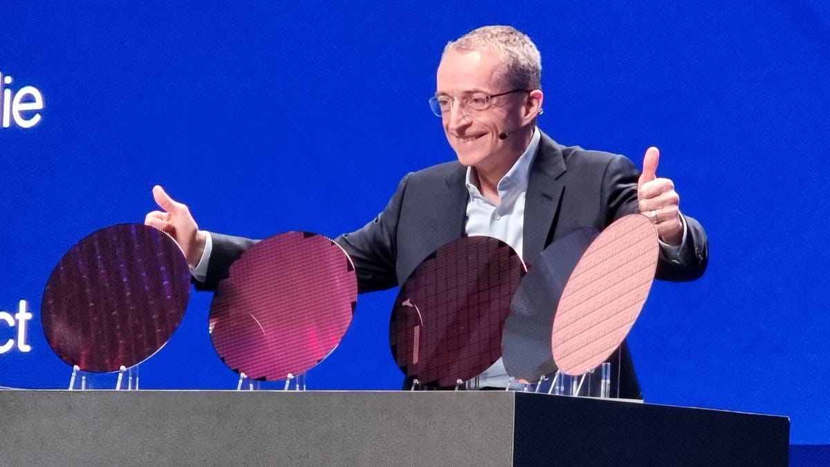
Pat: Both. We believe with 18A [we will have] the best transistors, backside power, and some of the evidence of that was described today by some of the EDA and IP providers. They're getting the best performance, the best area, the best power from 18A - so it’s the best process technology. Then, we’re taking our products, and I’m pushing our products on the leading edge of that. Clearwater Forest, our next-next generation server product for 2025, we already have that in fab now. Panther Lake, our 2025 client product, is already in fab at this point. So we’re pushing the envelope to leverage those process technologies and packaging technologies to build the best client and server products as well.
So yes, we’re on the path to be back to leadership with process technology, with our foundry offering that we present to customers, and the best products in the industry. That’s the path that we’ve laid out, and everything is coming together. As I said in the keynote today, we're not done with this arduous track that we set for the company with the 5 nodes in 4 years and rebuilding our execution machine. But today was a pretty profound day. [We’re] opening the doors up, and we see the light at the end of that very challenging track. We [also] laid out what's next – Intel 14A, the new process variants, and a cadence of technologies and we got great industry resonance that yes, in fact, this whole picture is coming true.
Ian: Awesome, well thank you very much, and good luck.
Pat: Thank you, Ian.
Final Thoughts
A number of key points came through in Pat’s responses.
1. #2 Foundry is External Business Only
2. IPG (product) has to fight for IF business
3. IF has to fight for IPG business
4. Foveros+EMIB is comparable to CoWoS
5. 18A has to work for both IPG and IF
6. Leadership in 2025 means both foundry and product
That external business only comment allows us to make predictions.
In Q3 2023, TSMC was #1 with $17.25 billion in revenue, while Samsung was #2 with $3.69 billion. Intel, by contrast, reported $0.31 billion, technically the peak of IF reporting to date. For now, we’re under the impression that is a mix of packaging and licensing revenue, but doesn’t include any of the internal foundry business. In order to hit #2, that number will have to 12x, indicating that external foundry has to be a $15b a year business by 2030, or a 51% CAGR. Also, that’s still expected to be under half of Intel’s total foundry business. Even if we put it at half, that’s a $30b/yr foundry business, or $7.5b a quarter.
In order for Intel to reach #2 foundry on external by 2030, IF revenue total (internal and external) would be over a third of TSMC today ($19.6b), and compared to today, would be half of all Intel revenue ($14.2b in Q4 2023).
Taking Q3 2023 is perhaps a bit singular minded, especially as in Q1 2021, Samsung actually reported $5.58 billion in revenue for the quarter. We could do the math again, but suffice to say, Intel expects its foundry business to be a significant portion of the company by the end of the decade, and a lot of that business is to be on 18A.
Intel leaning heavily on 18A has me a little concerned – they have to prove it works to customers (Pat’s words confirmed as much), but also bring customers to 18A. Nodes are getting ever more expensive to build chips on – from scratch, analysts predict that even 5nm/3nm nodes cost hundreds of millions to develop a chiplet, let alone fab in volume whole products. It will be interesting to see if Intel can bring the economics of that down, in order to enable a wider audience access to its manufacturing, and subsequently packaging.
Over 2024, some of the strongest voices to listen to as to the state of 18A will be the EDA vendors and their customers. Intel mentioned all the big ones at their foundry event – Synopsys, Cadence, Siemens, and Ansys (who just got acquired by Synopsys). Intel can talk about a v0.9 PDK of 18A being ready, almost full release, but it’s going to be the software tools and those that use the simulation stacks who will determine if Intel’s foundry offering can at least reach parity in usability compared to the rest of the industry.
I still need to go through the Foundry event and the announcements, and provide some insights. I have a long plane ride later today, and will crack on with that article for you.