
An Interview with AMD CTO Mark Papermaster
The Future is Faster Than Anyone Expected

If you rewind the clock ten years, AMD 0.00%↑ was not the company it is today. Zen had not yet shipped, EPYC was still on the roadmap, and the idea that AMD would be competing at the top end of CPUs, GPUs, and AI infrastructure simultaneously was far from consensus thinking. The last decade has seen one of the most aggressive technical rebuilds in the semiconductor industry, spanning core architecture, chiplet strategy, packaging, foundry partnerships, and now full rack-scale system design. That transformation did not happen in a single product cycle. It required long-term infrastructure bets, multi-generation execution discipline, and a willingness to absorb risk years ahead of visible results.
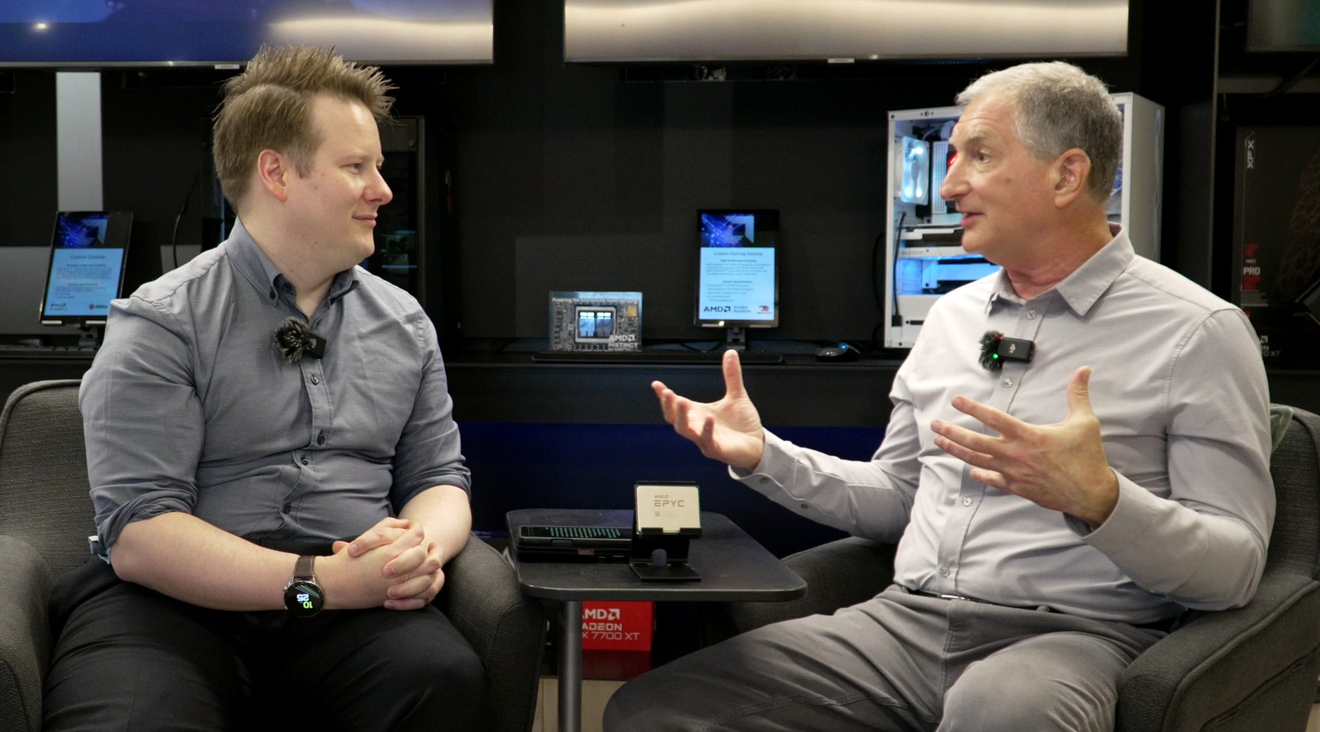
Joining me for this conversation is Mark Papermaster, AMD’s Chief Technology Officer and EVP. Mark has been at AMD since 2011 and has overseen much of the company’s modern engineering strategy, from the early Zen turnaround to Infinity Fabric, 3D V-Cache, Instinct GPUs, and the company’s recent push into rack-level AI platforms. In this interview, we talk about what changed inside AMD over the past decade, how engineering culture and roadmap planning evolved, where AI is reshaping chip design itself, and how AMD is thinking about power scaling, optics, cooling, and modular system architecture going forward.
The following is a transcript of the video interview embedded above. Phrases have been adjusted slightly to improve readability.
Ian Cutress: If I go back through my memory we first met in 2016 at IFA in Berlin, at a time when AMD wasn’t the big behemoth it is now. We were discussing the ins and outs of the market at the time. Given that you now have Ryzen, EPYC, and Instinct, the major product lines driving the company forward, what would you say has changed the most inside the company?
Mark Papermaster: I love that you go back to when we met in Berlin, almost 10 years ago, because it is a perfect capture of our journey. I joined in late 2011, and two or three months later, Lisa Su came on. She ran the business, I ran engineering, then Lisa became CEO two and a half years later. People didn’t realize in that period of time, up until when you and I spoke in 2016, of all of the building that had to go on to create a chip infrastructure that could be there for the AI era.
When you and I spoke, I don’t think almost anyone believed we could be a player in the industry. What I loved about when you and I chatted is you were very receptive; you follow the industry. You were asking, “Why do you think this new CPU, Zen, could compete?” and we talked about the different segments of the market and where it would go. In fact, it did play out that way, and we’ve had a chance to stay in touch over the years.
What has changed in that period of time is that visions turned to reality, both for the industry and certainly what the game plan that we set out to do at AMD. We set out to be a very agile competitor, offering not only CPUs and GPUs but other key hardware and software IPs to be able to be a solution provider, to be able to listen to customers. We now have an incredibly broad portfolio.
What’s happened in the industry since you and I spoke? That vision played out. It was a little bit different: in 2016, we probably all thought the Meta world would be more advanced than it is. We thought that was probably a bigger segment than it is, but we were very much talking about how disruptive AI would be. It has been all of that and more. For the most part, our vision of the industry and our vision for AMD has played out as we thought, but moved even more quickly than we imagined.
Ian Cutress: We’ve obviously had lots of discussions. I speak with the architects, and every time we talk about designing a chip, we have this two or three-year cycle, but then you have five and seven years of pathfinding and working with foundry partners, for example. Going back to then, how much of a “smoke screen” do you think the success of the first couple of generations of Zen was, relative to where the projected nature of the business was going to go?
Mark Papermaster: If you think about what we did with the first generations of Zen - we launched Zen in 2017, it came out in EPYC Servers and Ryzen PCs. You call it a “smoke screen”; I don’t use that analogy. I call that our proving ground years for the first two generations. The questions were: Is AMD for real? Is the value they’re providing real? Will they be a sustained innovator? Will they show up every cycle? Are they that true competitor bringing leadership performance, or are they a flash in the pan?
Ian Cutress: Before the success happened, you obviously have to project where you’re going. Everything’s hyper-accelerated now, but back then - and this is why I say “smoke screen” - at some point, you have to put the pedal to the floor. Was there any of that, or were you able to accurately work with customers and partners at the time to model where you expected to be?
Mark Papermaster: We had our pedal to the floor the entire time! You can’t do anything in this industry but move at your absolute best pace. When we launched Zen, we had banked the turnaround of AMD on having not just a competitive but a leadership processor. It took three generations to hit the knee of the curve on our Zen processor capabilities. Prior to Zen, the core had big gaps in competitiveness. The first generation added 42% instruction per clock.
Ian Cutress: I remember that presentation. It’s one of my key memories.
Mark Papermaster: It brought competition back to x86 CPUs. Since then, we’ve had double-digit IPC gains - significantly, 15% to 20% IPC every generation. So, no slowing down. By the time we hit the third generation Zen, everyone realized: “Wait a minute, AMD is a different AMD. They’re here every generation. They’re delivering exactly what they promised when they promised it”. That’s when our market gains started to really grow.
That’s a turning point for AMD - everyone saw the knee of the curve on technology capabilities and the financial results that came with it. We had always planned to start with CPUs because there’s no barrier to adoption; x86 is x86. If we delivered leadership, it would sell. People didn’t see that we had a GPU effort running in tandem to grow gaming graphics with Radeon, and we’ve always been very focused on AI and bringing GPU compute to market.
Ian Cutress: You mentioned double-digit gen-on-gen performance consistently. It’s the question that gets asked every five years, but given Amdahl’s Law, given Moore’s Law and Dennard Scaling, do you see a limit anytime soon in that raw single-core performance, or are we going to end up being workload dependent?
Mark Papermaster: I love that you asked that question because you’ve asked me that in every interview.
Ian Cutress: I expect everybody asks you that in every interview!
Mark Papermaster: It’s a common question - I love this question. It’s because I never cease to be amazed at the innovation of our engineers. Our CPU team is now a storied team under the technical leadership of Mike Clark. He coined the name Zen.
Ian Cutress: He told us he was called the “Zen Daddy” internally last time.
Mark Papermaster: He’s called the “Zen Daddy” - but it’s not just Mike, it’s the whole team around it. I could not be more excited with where our CPU roadmap’s going. Yes, we’re getting less out of every technology node, but we have an incredibly deep co-optimization with TSMC. For 2-nanometer, we are the very first customer of TSMC - the first tape-out that they received. We highly optimized around that. Although we’re not getting the same energy efficiency gains, we are getting density gains, and that’s very important to drive TCO forward.
You’re going to continue to see yet more density of cores. However, you can’t just bank on density of cores; you have to think about how you’re architecting to keep that balance of CPU computation, memory, and I/O. You need to make sure you have really efficient multiply-accumulate, because AI is everywhere, and everyone still has fleets of CPUs because you have all your legacy workloads. It’s not like they all go to a GPU; they’re going to be around for ages.
We are very excited about how we have modified our AVX engine. Your listeners know we have a dedicated AVX engine. We already run native 512-bit wide, and it’s already a good inferencing engine; it supports VNNI. Then, going forward, you’ve seen we said publicly in our work with the x86 advisory group that we have what we call the ACE engine. It’s an advanced, very flexible inferencing capability that we’re building into Zen 7 and beyond. It’s a super exciting future of CPU computation - not just performance per watt per millimeter squared, but also how you blend in inferencing capability and how you make sure it works seamlessly with the GPUs for heterogeneous computing.
Ian Cutress: Going back a little bit to the beginning, you’ve been at AMD now 15 years, going through that Zen, EPYC, and Instinct ramp. Has there ever been any situations where you’ve had to choose between an A or a B, and perhaps regretted the decision, or actually realized it was really good you did this over that?
Mark Papermaster: Of the latter, there are many decisions that we looked back and said were the right ones. There’s a few that were wrong for sure. But the biggest thing that we did right was the investment, even before we started the Zen core, in what became publicly our Infinity Fabric. It’s our network-on-chip link technology, and it was game-changing for AMD. You could build the best CPU and GPU, but if you can’t connect them seamlessly so they can scale and you don’t create bottlenecks, it doesn’t matter.
We started that investment in 2012, and we’re on our fifth generation of that fabric now. That’s been massively enabling. At the time, it was hugely disruptive - people quit the company. They felt it was the wrong way to go; we had top leaders just get up and leave.
Ian Cutress: I remember Mike saying that.
Mark Papermaster: That was an absolute decision that was game-changing. I’m not sure we would have made that decision if we weren’t in a position to make big bets.
Chiplet technology was a huge corporate bet. It’s paid off incredibly handsomely. In 3D stacking, we’re still the only one in mass production. Think about a gaming chip that has our SRAM or 3D V-Cache; for four years, it’s gone unchallenged because of bringing that memory locality.
We support what I call “healthy contention” in our engineering culture, where people throw rocks at different ideas and we can debate it professionally to make better decisions. We haven’t had huge misses; we haven’t had any micro-architectural visions that we’ve had to say, “Oh, we were just kidding, we’re not supporting that”. The misses we’ve had, if we’ve had something that caused a spin of silicon because of a late-breaking bug, we try to minimise that - we run a deep ‘lessons learned’ on it and adjust our methodology so we don’t repeat it. It’s built into our culture.
Ian Cutress: I remember the story Mike was saying about how the first spin that came back from Zen 1 could only work under sub-zero cooling, and some of the learnings had to be made at that point.
Mark Papermaster: Yeah, we absolutely had some issues on the first pass, but guess what? We worked around each one of them. That’s another thing: you have to build in resiliency. We have reliability, availability, serviceability architected in for robust operation. What people don’t realize is we have a ton of diagnostics and fungibility built in so that if there is something that got through, we can work around it. If it’s found late and it’s in production-level silicon, we can have a very robust production patch so that from an end customer, there’s no loss of functionality.
Ian Cutress: How important is it that an A0 has to work ready for commercial use? And how often do you hit that?
Mark Papermaster: For our GPUs, almost every cycle the A0 is the production target because GPUs are imminently programmable. They’re forgiven that way. CPUs, we’ve typically always designed with two passes in mind, but that’s changed going forward for two reasons. One, it’s an immense cost to build a mask set - so many millions of dollars for each mask set. Part two is building the test samples, because you need to really test across thousands of samples, and that’s also immensely expensive. We need across our whole portfolio to have first-time right.
The great news is AI has now come along, and we’re making great strides with AI across physical design, but where I’m most excited is actually design verification. We’re getting great agentic processes that are improving our coverage. We’re finding bugs earlier. We invested years ago in deep emulation technology - it’s not only important for us to get our designs right but that our own FPGAs are used!
Ian Cutress: How many of those machine learning tools in design and verification are coming directly from your EDA partners versus being built internally?
Mark Papermaster: It’s a mix, roughly half and half. If you look at the synthesis flows and the place-and-route flows, those we absolutely deploy our EDA partner solutions because they’re heavily investing there. But the other half where we have to really invest is our knowledge. It’s the agentic flow - how you take the smarts that you have. We’re a 55-year-old chip design company, and we have the most advanced packaging capabilities and some of the most advanced thermal cooling and power delivery. Those things impact the design itself.
You don’t just 3D stack; you architect for 3D stack. We had to create capabilities to make sure we didn’t have hotspots. So, where we’re cutting edge, we’ll develop the capability that we need. Going forward, we’re going to use the best the industry has to offer, but use our agentic flows with the knowledge capture over many years.
Ian Cutress: Some of the audience may not realize that you actually spent 26 years at IBM. You were working on a variety of things, including IBM Power. The tools we’ve just spoken about are obviously very new. Are there any common threads you can draw from those 26 years of experience that have come through your career to today?
Mark Papermaster: I was so lucky to start when I did. It was early ‘80s when I graduated and started with IBM. I started with a small renegade team that was tagged to create IBM’s first NMOS and then, two years later, their first CMOS ASICs. There was no EDA industry then. Our customer at that time was the IBM mainframe, which drove tremendous advances in technology. I learned to make multi-chip designs even back then.
I started as an analog person, then quickly went into digital and microprocessor design, and led Power microprocessor design. Analog taught me that you can never lose sight of the physics. Even though you have all the advanced analysis tools, it always came back to: Does the physics make sense? Is the science behind it sound?
What it really taught me from early on is the importance of cross-disciplinary innovation. It was the dawn of the EDA industry so it was bringing in advanced tooling and automation into chip design. Because we were a small integrated group, we had to work closely with the fab, so co-design with the foundry. I was ‘probes down’ on wafers, taking measurements.
The lessons from the ‘80s and ‘90s couldn’t be more applicable than today. Think about why BiCMOS changed over to CMOS: because BiCMOS drove too much power. Here we are running up against power limits again and having to innovate through those walls. The lesson I took away is, anytime someone tells you, “We’re dead,” “there’s a barrier,” or “Moore’s Law is dead.”, it’s the innovation that rules. We find ways to move around those barriers and provide end customer value.
Ian Cutress: So, Moore’s Law is not dead?
Mark Papermaster: Exactly!
Ian Cutress: It’s interesting you bring up your experience like that because a person we both know, Philip Wong at Stanford, has often lamented the fact that students today don’t have the same opportunities, or that the jobs in the industry aren’t being pivoted more towards chip design and physical design. Is there any opinion you have on ways that we can change that?
Mark Papermaster: I actually just saw Phillip and in the last couple of weeks we chatted about this. There actually is starting to be a return to hardware interest. Everything had shifted to software, but we are now seeing more students interested in hardware. But, Ian, it’s completely different now. We are promoting an AI-native approach to chip design at AMD. It’s thinking about chip design with AI as your right hand - just like you wouldn’t go anywhere without your phone - it’s an indispensable tool. AI is a productivity tool, and to reimagine chip design as AI-native from the outset is going to be incredibly disruptive over the next five-plus years. I think how we practice chip design today is going to completely change. Of course, we’re aiming for first time right - the kind of computation we’re building up to do AI training, that same computation can do AI for science. It’s going to disrupt the industry - we’re going to be able to get a much tighter marriage of silicon to algorithms.
Ian Cutress: Does that not create a risk of if the algorithms change, the silicon is worthless?
Mark Papermaster: Well, that’s why we continue our investments in general purpose CPUs and GPUs! People always jump to the conclusion that because custom design gets 40% more performance on a given workload, everything will shift there. Actually it doesn’t, and for the very reason that you stated - there’s a constant change of algorithms. So, you’re always going to need general purpose computing.
We believe that the tent is so large that there’s room for tailored specialized solutions even while you need the general programmability going forward. We have FPGAs so you can prototype and adapt to the latest algorithms. And for big customers that need a tailored version of silicon, we’re happy to do that and leverage our advanced packaging and foundry partnerships.
Ian Cutress: You’re saying that this tent is very broad, and one of the things that AMD’s done this year (2025) has been acquisitions - I think almost a dozen companies, several thousand employees, most of which have fallen under your organization. The question then becomes, does AMD have enough? Will there ever be enough engineers?
Mark Papermaster: It’s changing. First of all, as CTO, I work with all the teams. I’m very fortunate to have that role, and when you look at the skill acquisitions we’ve done, we’re very focused. Most of it has been AI model development, and a set of skills we needed with photonic and optical development. But the biggest acquisition this last year was ZT Systems, which gave us true rack scale design. You don’t have to look beyond next year’s Helios rack - we showed it off at OCP this year, and you can see the benefit of that tight partnership. Our competitors who looked at it said, “Wow, that is a true co-design”.
Going forward, you need deep co-design with the foundry. Now, for true AI training and large model inferencing, you have to have that same partnership with the top hyperscalers and model developers. We’ve earned that seat at the table. To optimize, you have to be skilled all the way through rack design. For the biggest AI compute capabilities, we now provide rack reference designs.
Ian Cutress: How much of that Helios design was done pre-acquisition, and was ZT Systems involved in that at all?
Mark Papermaster: They were. We were on a path to acquire, and it takes about a year to close these things. We created a set of agreements; the way it works is they have to be able to survive if the acquisition doesn’t go through. We put all that in place and created that deep co-design partnership. If you go back in time, we had already been working with ZT for years, and got a strong appreciation for their design and manufacturing capabilities. We already had a set of agreements in place. What you see in Helios is a result of true co-design.
Ian Cutress: Did that accelerate when money got involved?
Mark Papermaster: You say money, but what is money? It’s about having a leadership AI cluster design. Everyone knows the industry is going to quickly, so the carrot out there is huge already.
Ian Cutress: Going back to POWER, we went through a time of being shocked at 90 watts per core, 120 watts per core. Now we’ve got multi-core coming along: 128 cores, 192 cores, and 500 watts per chip. We have AI chips hitting a kilowatt, two kilowatts, and you’ve seen the same predictions I have going to six kilowatts to ten kilowatts per chip. From an engineering perspective, does that worry you?
Mark Papermaster: It’s like I said earlier - it drives different innovation. Some people look at it and say, “We’re clearly going to hit a power wall, and innovation will stop”. No, it drives innovation.
We are shipping 750-watt GPUs today, on our way to kilowatt and two kilowatt designs and beyond. It’s spurring tremendous innovation. In the last two weeks I’ve met with startups and seen university research on heat spreading and heat removal technology. At IEEE last month the lead article was on a diamond heat spreading technology that’s pretty amazing. So there’s a lot in the development pipelines that will help here.
What you’re going to see in the immediate term is those that need dense clusters will all adopt tightly integrated liquid cooling. That’s becoming a de facto standard for dense racks. It’s a problem to overcome; but it’s not a barrier, but you have to co-architect it.
Ian Cutress: The funny thing is speaking about IBM before, they actually did a lot of work in the ‘90s on intra-chip cooling.
Mark Papermaster: Oh my! Those mainframes I referred to earlier - each chip sat on a “pogo stick,” which was a heat removal thermal conduit. If you take inflation into account, that was a pretty expensive design approach! But it just tells you: engineers innovate; engineers solve problems. The new approaches will be much more economical than back in the ‘90s to do equivalent highly efficient heat removal.
Ian Cutress: You’re talking about these racks being tightly coupled co-design. But if we go back to the IBM mainframes of the ‘80s and ‘90s, the irreducible unit was the mainframe. When we look at rack scale today, we have CPUs, and GPUs, and optical connectivity. We designed them in a different way.
Mark Papermaster: Today, it’s much more modular than it was at that time. We’re committed to modularity at AMD because it expands our addressable market. If we tailored the GPU or CPU compute core only for data center computation, we couldn’t address enterprise needs, edge computing, or all the way down to PCs. We are running 100-billion-parameter models on AIPCs today.
From our perspective, we wake up every morning thinking about how to architect across that scale. We have people that wake up every day thinking about vertical optimization, focusing on rack scale. Then we have other people who are thinking horizontally. They create that healthy contention and say, “I love what you’re doing for rack, but if you did a slight change, we could derive that in a very fast way to address the other markets we serve in AMD”. It goes back to our conversations back in 2016 - that modularity is a huge part of our history today, and it’s an even bigger part of our opportunity going forward.
Ian Cutress: When we look at the next several years, everyone’s talking about bandwidth, whether that’s intra-chip, chip-to-chip, or chip-to-memory. One of the things I’ve been focusing a lot on is the optics realm, especially co-packaged optics. The route to optics is very top-of-mind for the big GPU players. What’s your opinion there, and how should we frame it mentally?
Mark Papermaster: The way to think about optics is: why is it only prevalent in scaling out massive clusters in data centers, and not scaling up the densest clusters? The reason has been cost. Copper has done the trick. Helios is a 72-GPU node design using copper; it’s cheap, reliable, and you have to architect that in, but it works great. But as you go beyond 72 nodes and start getting the scalability into thousands - thinking of Mixture of Experts approaches - you want bigger and bigger cluster sizes.
The good news is, photonics in the next several years will tip over to be economically viable. The supply chain is coming up. You will see photonic solutions phase in where you need very, very dense nodes. But copper won’t go away because you have such a range of solutions. Think about all the enterprises out there that do not need foundational model training. Think of photonics as coming on board in the next three years, all the pieces of the supply chain coming together, starting at just the biggest clusters.
Ian Cutress: From a technical standpoint, can you design a product that can switch in and out optics versus copper, or do you have to go down the optical route for definite?
Mark Papermaster: You can architect for both. You can architect in flexibility.
Ian Cutress: Most of the discussion today is chip-to-chip, but we’re seeing some solutions today talking about optics to more banks of HBM, a sort of chip-to-memory expansion. How much of that is on your radar?
Mark Papermaster: Well, we follow it all. Celestial.ai has just announced that Marvell will be acquiring them, and they’re working on solutions like that. We think that’s a fine solution, and congrats to David and the team, we think it’s a fine solution. AMD is all about an open ecosystem. We encourage all these types of innovations because it gives our customers more choice. We’re not about a solution that’s proprietary and is all AMD top to bottom. For us, it’s about getting the best compute elements out and having multiple partners that can piece that solution together. The next 3 to 5 years are going to be very exciting around photonics.
Ian Cutress: How much has stress increased moving to this yearly cadence on compute?
Mark Papermaster: We were already on an annual cadence for PCs and consumer gaming. Our EPYC CPUs have largely remained on an 18 month cycle. We knew what it would take to move to an annual cadence. But the pace of AI is torrid, and it’s driven by customers who just need that type of improvement. Whether it’s new math type formats or elements of that nature, it just needs that pace, and that’s what we’ve done. We found we had to understand the pinch points and beef up staffing in certain areas. It’s where we’re focused on applying AI into our chip design practices - on the chip points that facilitate that annual cadence.
Ian Cutress: That’s obviously very customer-driven. How does that affect your pathfinding? How do you still innovate when you’re on the treadmill of getting designs out so quickly?
Mark Papermaster: That’s a common concern. Some companies have said, “We’re going to have a half a day every Friday for innovation,” but I haven’t found that to be effective. What we have found is you have to have innovation built into the design process. So rather than rush that design phase up front, we have pathfinding teams, and it starts in research. We have a very strong research team, and it doubled in size when we acquired Xilinx. Xilinx was also committed to an open ecosystem just like AMD, so that came beautifully. So pathfinding starts there. If you think about the most advanced work on CPU, GPU, and AI algorithms, it’s in a five-year plus timeframe for the research team.
But we don’t just have an ivory tower research team that’s just looking at five years and beyond, part of that team is in the three-to-five year, and they’re working with the development teams that are getting out the next generation Zen CPU or Instinct GPU. Then, at the high-level design phase, we want to give the teams the time to make sure that they have the right innovations to be competitive. We have a well oiled roadmap process, it’s one of the things that Lisa and I put in place back around the time we first talked, or even earlier. We put in a philosophy of these ideas also solving a customer issue and having a business team to pair with them to ensure it also matches a market need. We give our teams the agility to innovate, but when we approve a project, it has to have the rigor behind it. We need our projects to all deliver and return what they promised to the company.
Ian Cutress: For 2026, can you give the audience the thing that you’re most looking forward to?
Mark Papermaster: 2026 is going to be really exciting from a couple of fronts. At AMD, we couldn’t be more excited about what our next-generation Instinct GPU brings, because with that Helios rack, it brings us smack dab into full-scale training and inference. We support training today, but it’s to the thousands of nodes, not the hundreds of thousands of GPUs that we will have the capability to support.
From an industry standpoint, it is incredibly exciting because, just like we’re seeing with our chip design, with AI really starting to have high-impact agentic processes coming online. I’m talking to more and more customers on broader enterprise that are seeing that impact. I think in 2026, we start to see yet more use that we all have in our day-to-day lives where AI becomes absolutely indispensable.
Additional: Mark has his own podcast, speaking with industry luminaries. It’s worth checking out.
https://www.youtube.com/playlist?list=PLx15eYqzJiffUsiIhsSM_q-ukoW5_3YJ1

“The next 3 to 5 years are going to be very exciting around photonics” - it’s coming faster than Mark predicted: https://bit.ly/4kD58lq
Thank you for the interview. I always enjoy listening to Mr. Mark Papermaster, or anyone else from AMD.